

| SID Receiver overview |
| Synoptic |
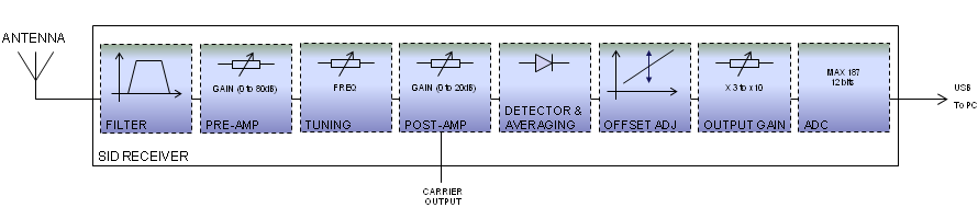
The basic principle of the SID receiver is to measure the amplitude of a VLF station and to convert it to digital data.
The signal from the antenna (usually a loop antenna) is filtered out to limit the signals to the frequencies of interest in the VLF and lower-LF frequency range.
The RF pre-amplifier section is built around one non-inverting amplifier with a gain of 21 and two inverting amplifier stages with gains adjustable between 0 and 25.
The signal is then filtered in the tuning section. The MAX275 is a continuous-time 4th-order active filter. The MAC275 is configured as a bandpass filter; center frequency, gain and Q are adjusted by resistors.
The following section is the RF post amplifier. It has a gain adjustable between 0 and 10. A buffer provides an optional carrier output with a 50Ω impedance.
Then, a full-wave rectifier and peak detector is used as a linear detector converting the RMS value of the VLF station to a DC voltage level. This level is averaged (default time constant around 1 minute) to produce a signal strength value.
DC offset can be applied to the signal strength value, before further amplification in the output amplifier section (selectable gains of x3.25, x4 and x10).
Finally, the analog to digital conversion is performed by the 12-bits ADC MAX187.
The interface between the MAX187 and the computer is done though an USB port.
The design has been highly inspired from the SID monitor of the Stanford Solar Center.
The schematics for the SID receiver as well as the bill of material is available here:
 SID Receiver v1.1 schematics SID Receiver v1.1 schematics | (application/pdf, 116Kb, 05 Mar 2011) | |
| SID Receiver v1.1 power supply schematics | (application/pdf, 20Kb, 05 Mar 2011) | |
| SID Receiver v1.1 bill of materials | (application/pdf, 88Kb, 10 Apr 2011) | |
| Values of the frequency tuning resistors | (application/pdf, 45Kb, 17 Mar 2011) | |
| SID Receiver Assembly Manual | (application/pdf, 15609Kb, 12 Jul 2011) |
To view those files, you need a PDF viewer such as SumatraPDF (Windows):
 or Adobe® Reader® (Windows, Mac, Linux):

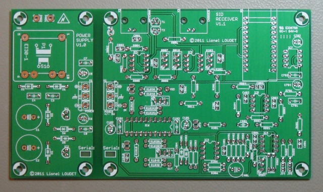
| Printed Circuit Board |
A small quantity of high quality printed circuits boards for the SID receiver have been manufactured.
The author offers those boards for 30 euros plus shipping costs.
Please contact me ![]() for availability.
for availability.
The printed circuit board is out of stock. Production of another batch is not planned.
Here is a picture of the board:
| Tuning |
| Assembly |
Last step is to put the PCB in a metallic box with the transformer, fuse and power switch.
See the pictures here below for assembly example:
") | ") |
| Data Transfer Protocol |
Here are some details regarding the data transfer protocol between the MAX187 and the RS-232 interface.
The MAX187 signals are connected to the following RS-232 pins:The RS-232 standard defines the positive voltage levels for logic one and negative voltage level for logic zero.
Protocol is detailed in the following documents:| • MAX187 Datasheet | |
| • Maxim application note 827. This note contains a C code example. |

|
SID monitoring station by Lionel LOUDET is licensed under a Creative Commons Attribution-NonCommercial-ShareAlike 3.0 Unported License. |
|
| Last Update: 20 Jul 2013 |
|
Apache/2.4.59 (Debian) |
|